Project Report on semiconductors || Class 12 physics project on semiconductor
Project Report on semiconductors:-
INTRODUCTION:
Most of the solids can be define into three classes: 1) conductor 2) insulator and 3) semiconductor (1) conductor: those solids can be called as conductor who have good electric conductivity property. Conductivity define by the presence of free electron. That means conductor have free electron by which it can easily conduct current. Example:- copper, iron etc. (2) insulator: those solid can be called insulator who have no electric conductivity. That means insulator have no free electron and hence they cannot conduct current. Example:- wood, glass etc. (3) semiconductor: semiconductor are those solid whose electric conductivity is between conductor and insulator. Semiconductor can conduct current in some particular conditions.
Theory:-
The energy band structure of the semiconductors is similar to the insulators but in their case, the size of the forbidden energy gap is much smaller than that of the insulator. In this class of solid the forbidden energy gap is of the order of about 1ev, and the two energy bands are distinctly separate with no overlapping. At absolute zero temperature, no electron has any energy even to jump the forbidden gap and reach the conduction band. Therefore the substance is an insulator. But when we heat the solid, this provide some energy to the atoms and their electrons, it becomes an easy matter for some electrons to jump the small (» 1 ev) energy gap and go to conduction band. Thus at higher temperatures, the solid becomes a conductors. This is the specific property of the solid is known as a semiconductor.

Effect of temperature on conductivity of Semiconductor:-
At 0K, all semiconductors are insulators. The valence band at absolute zero is completely filled and there are no free electrons in conduction band. At room temperature the electrons jump to the conduction band due to the thermal energy. When the temperature increases, a large number of electrons cross over the forbidden gap and jump from valence to conduction band. Hence conductivity of semiconductor increases with temperature.
- semiconductor can be divided into two types such as 1) intrinsic and 2) extrinsic
INTRINSIC SEMICONDUCTORS:
Pure semiconductors are called intrinsic semi-conductors. In a pure semiconductor, each atom behaves as if there are 8 electrons in its valence shell and therefore the entire material behaves as an insulator at low temperatures.
A semiconductor atom needs energy of the order of 1.1ev or more to shake off the valence electron. This energy becomes available to it even at room temperature. Due to thermal agitation of crystal structure, electrons from a few covalent bonds come out. The bond from which electron is freed, a vacancy is created there. The vacancy in the covalent bond is called a hole i.e hole is absence of electron.
This hole can be filled by some other electron in a covalent bond. As an electron from covalent bond moves to fill the hole, the hole is created in the covalent bond from which the electron has moved. Since the direction of movement of the hole is opposite to that of the negative electron, a hole behaves as a positive charge carrier. Thus, at room temperature, a pure semiconductor will have electrons and holes wandering in random directions. These electrons and holes are called intrinsic carriers.
As the crystal is neutral, the number of free electrons will be equal to the number of holes. In an intrinsic semiconductor, if  denotes the electron number density in conduction band,
  the hole number density in valence band and
  the number density or concentration of charge carriers, then
EXTRINSIC SEMICONDUCTOR:
As the conductivity of intrinsic semi-conductors is poor type, so intrinsic semi-conductors are of little practical importance. The conductivity of pure semi-conductor can, however be enormously increased by addition of some pentavalent or a trivalent impurity in a very small amount (about 1 to 106 parts of the semi-conductor). The process of adding an impurity to a pure semiconductor so as to improve its conductivity is called doping. Such semi-conductors are called extrinsic semi-conductors. Extrinsic semiconductors are of two types :
i) n-type semiconductor
ii) p-type semiconductor
i) n-type semiconductor

(black dot indicate "electron" and white dot indicate "hole")
When an impurity atom belonging to group V of the periodic table like Arsenic is added to the pure semi-conductor, then four of the five impurity electrons form covalent bonds by sharing one electron with each of the four nearest silicon atoms, and fifth electron from each impurity atom is almost free to conduct electricity. As the pentavalent impurity increases the number of free electrons, it is called donor impurity. The electrons so set free in the silicon crystal are called extrinsic carriers and the n-type Si-crystal is called n-type extrinsic semiconductor. Therefore n-type Si-crystal will have a large number of free electrons (majority carriers) and have a small number of holes (minority carriers).
In terms of valence and conduction band one can think that all such electrons create a donor energy level just below the conduction band as shown in figure. As the energy gap between donor energy level and the conduction band is very small, the electrons can easily raise themselves to conduction band even at room temperature. Hence, the conductivity of n-type extrinsic semiconductor is markedly increased.
In a doped or extrinsic semiconductor, the number density offree electron in the conduction band () and the number density of holes in the valence band () differ from that in a pure semiconductor. If is the number density of electrons is conduction band, then it is proved that
ii) p-type semiconductor

(black dot indicate "electron" and white dot indicate "hole")
If a trivalent impurity like indium is added in pure semi-conductor, the impurity atom can provide only three valence electrons for covalent bond formation. Thus a gap is left in one of the covalent bonds. The gap acts as a hole that tends to accept electrons. As the trivalent impurity atoms accept electrons from the silicon crystal, it is called acceptor impurity. The holes so created are extrinsic carriers and the p-type Si-crystal so obtained is called p-type extrinsic semiconductor. Again, as the pure Si-crystal also possesses a few electrons and holes, therefore, the p-type si-crystal will have a large number of holes (majority carriers) and a small number of electrons (minority carriers).
It terms of valence and conduction band one can think that all such holes create an accepter energy level just above the top of the valance band as shown in figure. The electrons from valence band can raise themselves to the accepter energy level by absorbing thermal energy at room temperature and in turn create holes in the valence band.
Number density of valence band holes () in p-type semiconductor is approximately equal to that of the acceptor atoms ( ) and is very large as compared to the number density of conduction band electrons (). Thus,
ELECTRICAL RESSITIVITY OF SEMICONDUCTOR:
Consider a block of semiconductor of length L, area of cross-section A and having number density of electrons and holes as and respectively. Suppose that on applying a potential difference, say V, a current I flows through it as shown in figure. The electron current ( ) and the hole current (
 ) constitute the current I flowing through the semi conductor i.e.
If is the number density of conduction band electrons in the semiconductor and  , the drift velocity of electrons then
Similarly, the hole current, 
From equation (i) I=
I= ........(ii)
If r is the resistivity of the material of the semiconductor, then the resistance offered by the semiconductor to the flow of current is given by :
R = r I/A ........(iii)
Since V = RI, from equation (ii) and (iii) we have
If E is the electric field set up across the semiconductor of unit cross section, then:
from equation (iv) and (v), we have
On applying electric field, the drift velocity acquired by the electrons (or holes) per unit strength of electric field is called mobility of electrons (or holes). Therefore,
Mobility of electrons and holes is given by :
Mobility of electron is  and mobility of hole is
Also,  is called conductivity of the material of semiconductor
The relation (vi) and (vii) show that the conductivity and resistivity of a semiconductor depend upon the electron and hole number densities and their mobilities. As and increases with rise in temperature, therefore, conductivity of semiconductor increases with rise in temperature and resistivity decreases with rise in temperature.
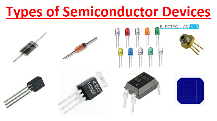
Now in modern age most of the electronics device is composed by semiconductor device as memory card, chips, pendrive, computer, mobile and so many digital instrument we use in our everyday life.


Comments
Post a Comment